
Browse by Stream
-
Engineering and Architecture
Exams
Colleges
Predictors
Resources
-
Computer Application and IT
Quick Links
Colleges
-
Pharmacy
Colleges
Resources
-
Hospitality and Tourism
Colleges
Resources
Diploma Colleges
-
Competition
Other Exams
Resources
-
School
Exams
Top Schools
Products & Resources
-
Study Abroad
Top Countries
Resources
-
Arts, Commerce & Sciences
Colleges
Upcoming Events
Resources
-
Management and Business Administration
Exams
Colleges & Courses
Predictors
-
Learn
Law Preparation
MBA Preparation
Engineering Preparation
Medical Preparation
-
Online Courses and Certifications
Top Streams
Specializations
- Digital Marketing Certification Courses
- Cyber Security Certification Courses
- Artificial Intelligence Certification Courses
- Business Analytics Certification Courses
- Data Science Certification Courses
- Cloud Computing Certification Courses
- Machine Learning Certification Courses
- View All Certification Courses
Resources
-
Medicine and Allied Sciences
Colleges
Predictors
Resources
-
Law
Resources
Colleges
-
Animation and Design
Exams
Predictors & Articles
Colleges
Resources
-
Media, Mass Communication and Journalism
Colleges
Resources
-
Finance & Accounts
Top Courses & Careers
Colleges
Get Answers to all your Questions


- #Medical
- #Maharashtra Common Entrance Test
- #National Eligibility Cum Entrance Test
- #Electronic devices
- #Physics
- #Class 12
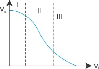
Transfer characteristics [output voltage (V0) vs input voltage (Vi)] for a base biased transistor in CE configuration is as shown in the figure. For using transistor as a switch, it is used:
Option: 1
In region III
Option: 2
Both in region (I) and (III)
Option: 3
In region II
Option: 4
In region I
Answers (1)
As we learned in
Transistor -
Three layered semiconducting device .
NPN or PNP
- wherein
1. Emitter is heavily doped
2. collector is moderately doped .
3. Base is lightly doped & very thin
For using transistor as a switch it is used in cut off state and saturation state only.
View full answer
NEET 2024 Most scoring concepts
- Just Study 32% of the NEET syllabus and Score up to 100% marks

